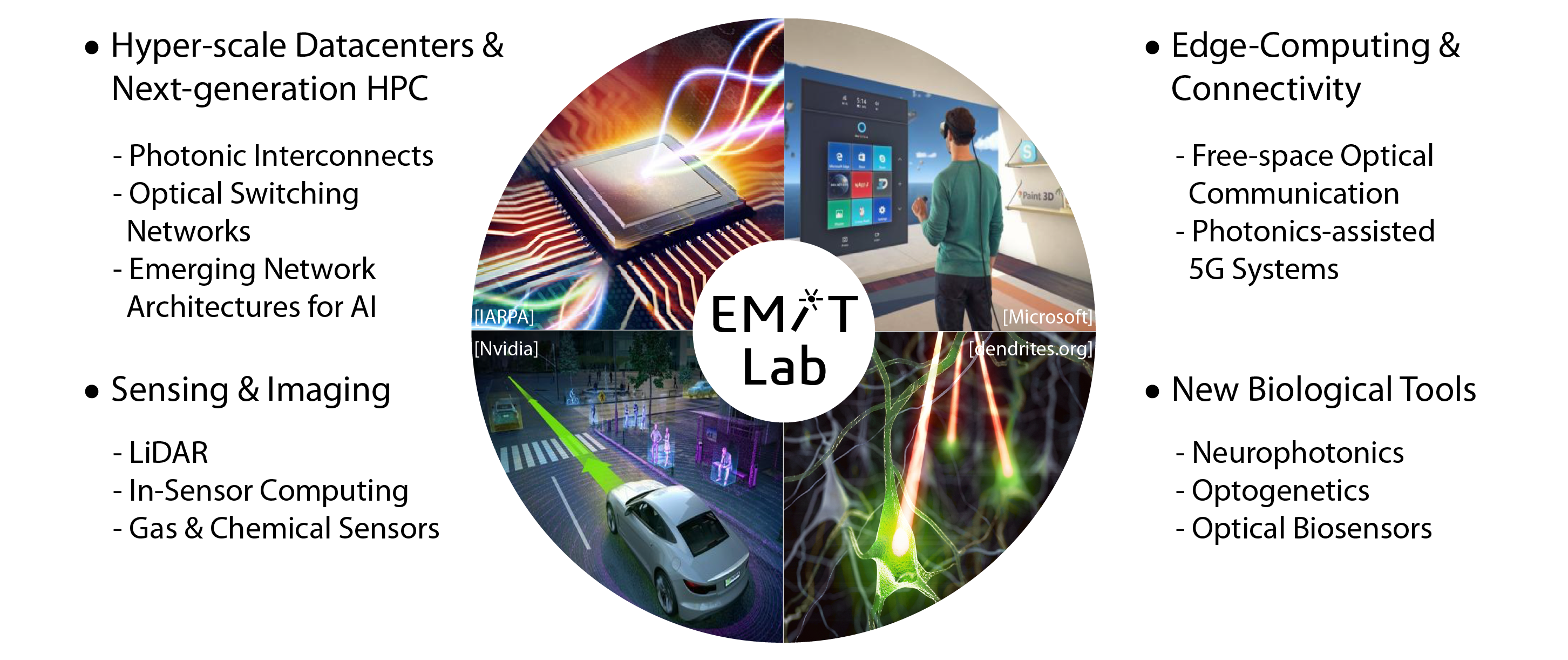
Our research aims to design and implement large-scale integrated systems by merging state-of-the-art electronics with photonics and other emerging technologies. These systems target applications in Optical Interconnects, AI Compute Clusters (scaling out/up), Non-classical & Quantum Computing, Cryogenic and Radiation-Hard Optics, Optical Imaging and Sensing, and Biomedical Devices.
Our group addresses all critical aspects of integrated system design, including system-level modeling and architecture, mixed-signal integrated circuits and systems, as well as post-processing and integration technologies. The guiding principle behind our integrated system approach is to enhance and leverage existing commercial CMOS technologies, enabling new functionalities and unprecedented performance for emerging applications. These enhancements include post-CMOS processing (fabrication steps completed after the chips are manufactured at the foundry), 3D integration, and “zero-change” approaches that repurpose existing materials within standard CMOS processes.
 As AI models grow in size and GPUs and AI accelerators become increasingly powerful, optical interconnects and networks are emerging as critical factors in determining the overall compute speed, energy efficiency, and capacity of data centers. Our research focuses on developing key technologies to address these challenges, including co-packaged optics, DSP-free/lite coherent optical links, and low-cost electronic-photonic packaging techniques for rapid prototyping. This work is supported by the NSF, SRC, Google, and the UW Clean Energy Institute (CEI).
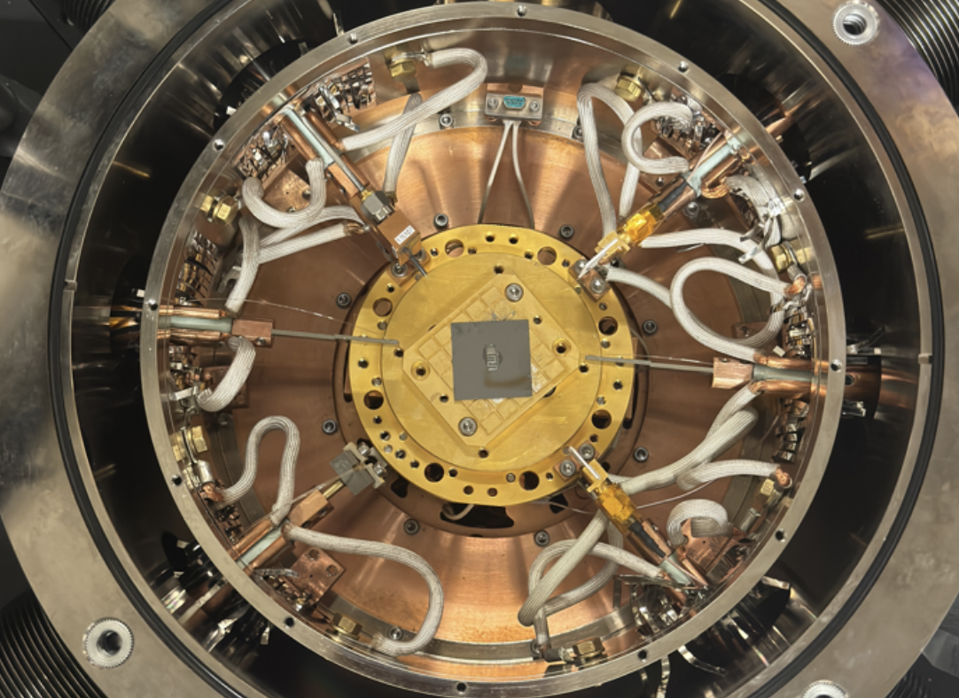 Cryogenic optical links are critical for future of quantum computers and high-energy physics (HEP) experiments. We are focusing on design and characterization of cryogenic (4K) photonics as well as mixed-signal high speed CMOS front ends for this aim. This research is supported by DOE and in collaboration with Fermi National Labs.
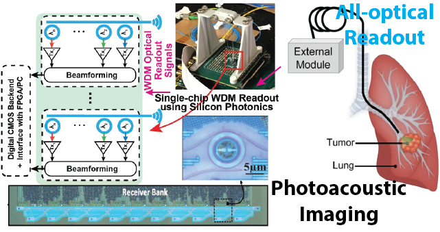 Silicon photonics has immense applications in optical methods for biomedical applications and neuroscience. We are currently focusing on developing new photonic devices for ultrasound detection as well as realizing all-optical readout and data acquisition (DAQ) for endoscopic/probe imaging applications. This research is supported by ARPA-H and we are in collaboration with Northeastern, Johns Hopkins & MGH to build photoacoustic imaging technologies for diagnostic lung cancer assessment.
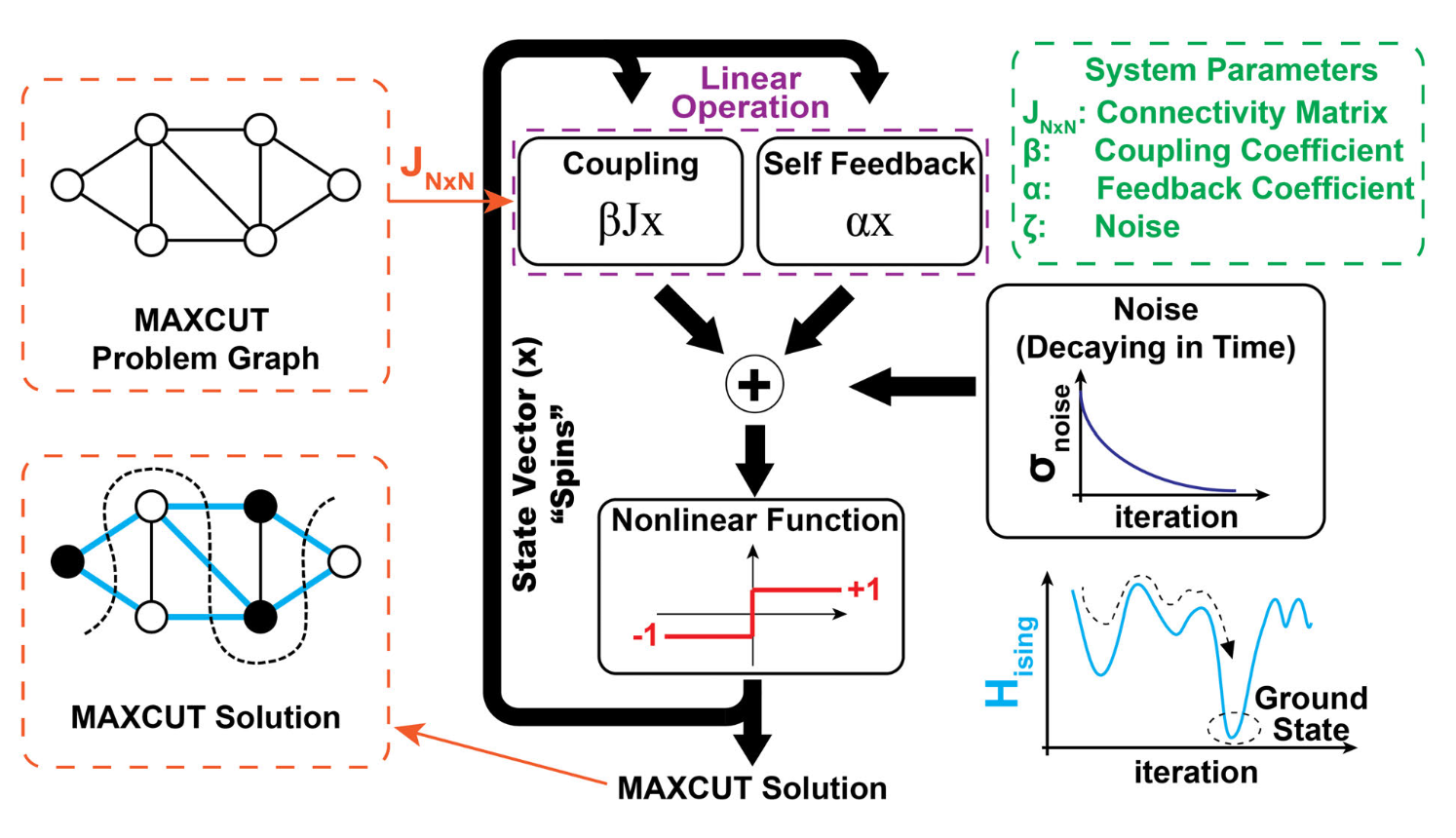 Combinatorial and discrete optimization problems are prevalent in fields such as artificial intelligence, supply chain management, and wireless communications. Ising machine is a quantum-inspired paradigm that cab offer a novel approach to accelerate these computations. We are focusing on building ultra-low power Ising machines with sub-microsecond latency in CMOS for edge applications in wireless systems.
 Generative AI can revolutionize the way we are design integrated circuit todays, impacting the future of CAD/EDA tools. In our group, we are working on using agentic AI methods to speed up the design time of mixed-signal and digital CMOS as well as photonic integrated circuits (PIC).
All-optical interrogation of cortical neurons enables simultaneous in-vivo readout and manipulation with single-neuron and single-action potential precision. This approach relies on Optogenetics and Calcium/Voltage imaging. In this work, both of these biological techniques will be miniaturized on a single implantable lens-less integrated system that can be wirelessly powered up and controlled. This system provides neural access to large areas of brain cortex bringing new opportunities to study brain circuits and building advanced brain-machine-interfaces.
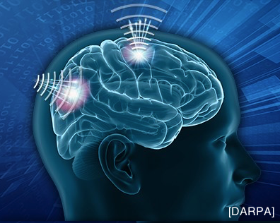
Mental control of robots and machines by human brain can be a reality in near future. We are building a noninvasive high-bandwidth brain-computer-interface capable of recording/stimulating neurons in the visual cortex with high spatiotemporal resolution for this aim. In this project, a single photon avalanche diode (SPAD) based imager array will be implemented to record neural activity using Near-Infrared (NIR) optical tomography. Here is a press release on the end goal of this project on Neuroscience News.
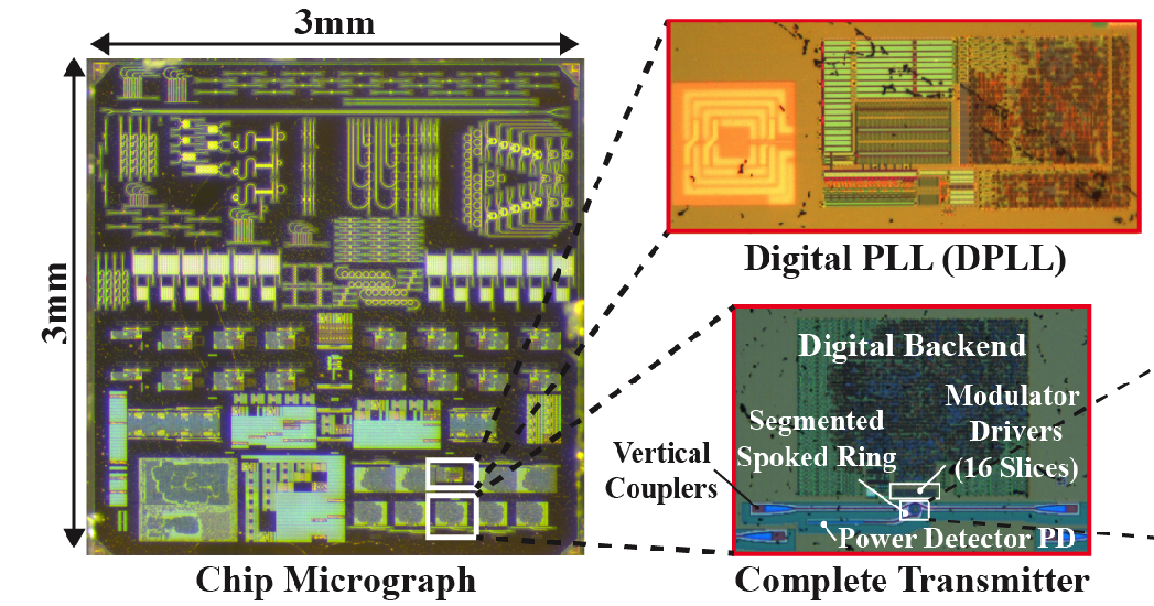
We have demonstrated the first 40Gb/s optical PAM-4 transmitter in an “zero-change” (unmodified) 45nm SOI CMOS process. This transmitter achieves modulator and driver energy efficiency record of 42fJ/b which is 2 orders of magnitude more efficient than industry workhorse MZI-based transmitters In this work, we introduced an Optical DAC based on segmented microring modulator structures and a thermal tuning control loop for multi-level ring-resonator based transmitters. This high-speed Optical DAC can be also used for optical arbitrary waveform generators (AWG) and RF-photonics applications.
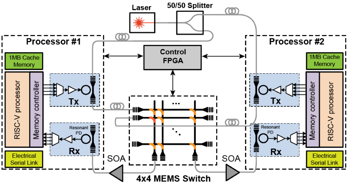
We have recently demonstrated the first dual-core processor SoC integrated with WDM optical I/Os. In this projects, we demonstrated an optical circuit switching network of these processor chips via a MEMS optical switch with microsecond switching time. This system demonstration is a promising solution to solve the electrical packet switching (EPS) scalability and energy-efficiency issue and enables novel architectures for emerging disaggregated and heterogeneous data-centers and HPC.
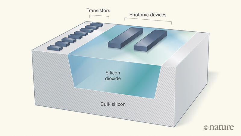
In order to realize the most energy-efficient and highest-bandwidth density interconnect across a range of applications, photonic devices need to be integrated as closely as possible to the most advanced transistors on a variety of chips designed mostly in a bulk CMOS process (e.g. processors, switches, memory chips, etc.). As a step toward creating a photonics process module that can be added to nanoscale CMOS process nodes, we demonstrated a polysilicon-based platform in a low-power 65nm bulk CMOS process in a 12” wafer foundry for the first time.
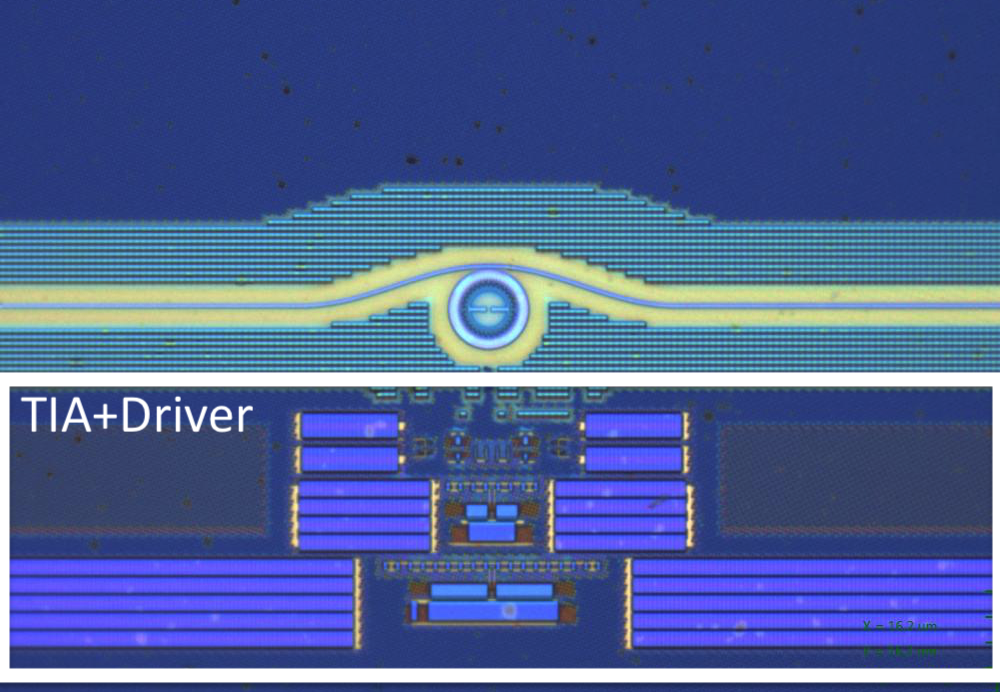
A monolithic photonic platform in an unmodified HKMG 32nm SOI CMOS process has been proposed in this work. This platform provides the fastest transistors monolithically integrated with photonic components. We showed high-speed O-band optical transceivers using resonant-based modulators and detectors with analog front-end circuits. Additionally, we exploited a new SiGe layer available in this process to improve the quantum-efficiency of resonant photo-detectors.
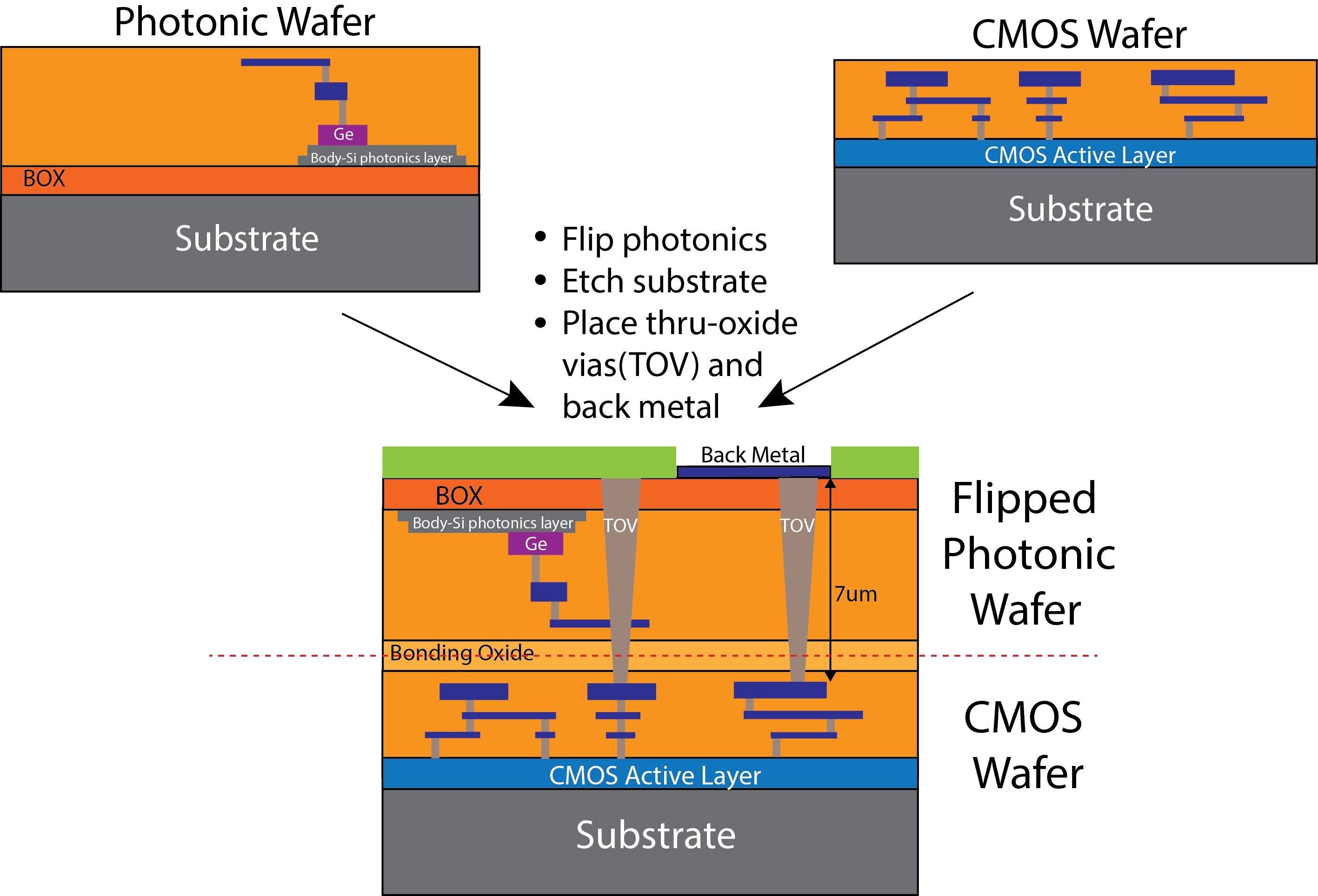
3D integration of electronics and photonics enables independent optimization of the photonic components and the CMOS circuits. We demonstrated for the first time a wafer-scale 3D electronic-photonic integrated platform, interfaced by the low capacitance (3fF/via) Through-Oxide-Vias (TOV) with 4μm pitch suitable for large-scale and energy-efficient electro-optical systems. This platform provides the densest 3D integration platform with the lowest parasitics among multi-wafer solutions.

Co-simulation and optimization of emerging integrated systems such as high-speed optical transceivers is a must to achieve the target performance and energy efficiency. This work proposes a new framework for designing high-speed silicon photonic transmitters by incorporating an accurate compact model for optical phase shifters, analytical models for photonic modulators and a new Simulink simulation toolbox. It allows us to explore the design trade-offs in depth for microring and Mach-Zehnder optical transmitters and compare their performances given the same set of technology and link constraints. Simulink Toolbox
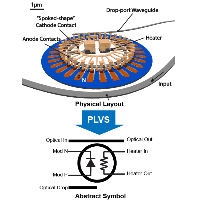
As the number of photonic devices in advanced electro-optical systems such as LiDARs, optical switches, SoCs with optical I/O, quantum optics chips, and etc. are growing fast, the need for a “photonic VLSI flow” is imminent. We have developed a photonic layout versus schematic (PLVS) tool which extracts photonic devices and their properties from the layout and compares with the desired design parameters for the verification. It is compatible with original CMOS foundry PDKs and can recognize both PDK devices and new photonic structures. Our approach can be extended to other silicon photonics technologies with similar device structures as well.